 SIMHUB
Package modelling
Read upstream EDA designs and use parametric tools for common package forms.
Chip & package multiphysics
Technology by SimWE
An integrated thermal, structural and electromagnetic simulation product for advanced chip packaging, developed on Simdroid’s shared architecture.
Discuss Simdroid-IC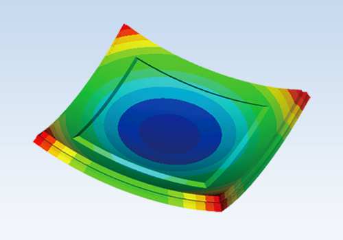
BUILT FOR YOUR WORK
Chip and package engineers assessing thermal performance, mechanical reliability and electromagnetic behaviour.
Read upstream EDA designs and use parametric tools for common package forms.
Investigate thermal, stress and electromagnetic effects within one workflow.
Review temperature, warpage and field distributions before refining the package.
AN EVALUATION WORKFLOW
Package geometry, materials, process information and loads.
Configure the required physical fields and their coupling.
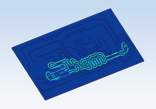
Examine thermal maps, deformation and electromagnetic results.
The workflow above is an evaluation outline. Confirm the required modules, interfaces and version for your application.
Product information from SimWEAPPLICATIONS IN PRACTICE
Discuss your package geometry, boundary conditions and target outputs with Simhub.
Plan an evaluation